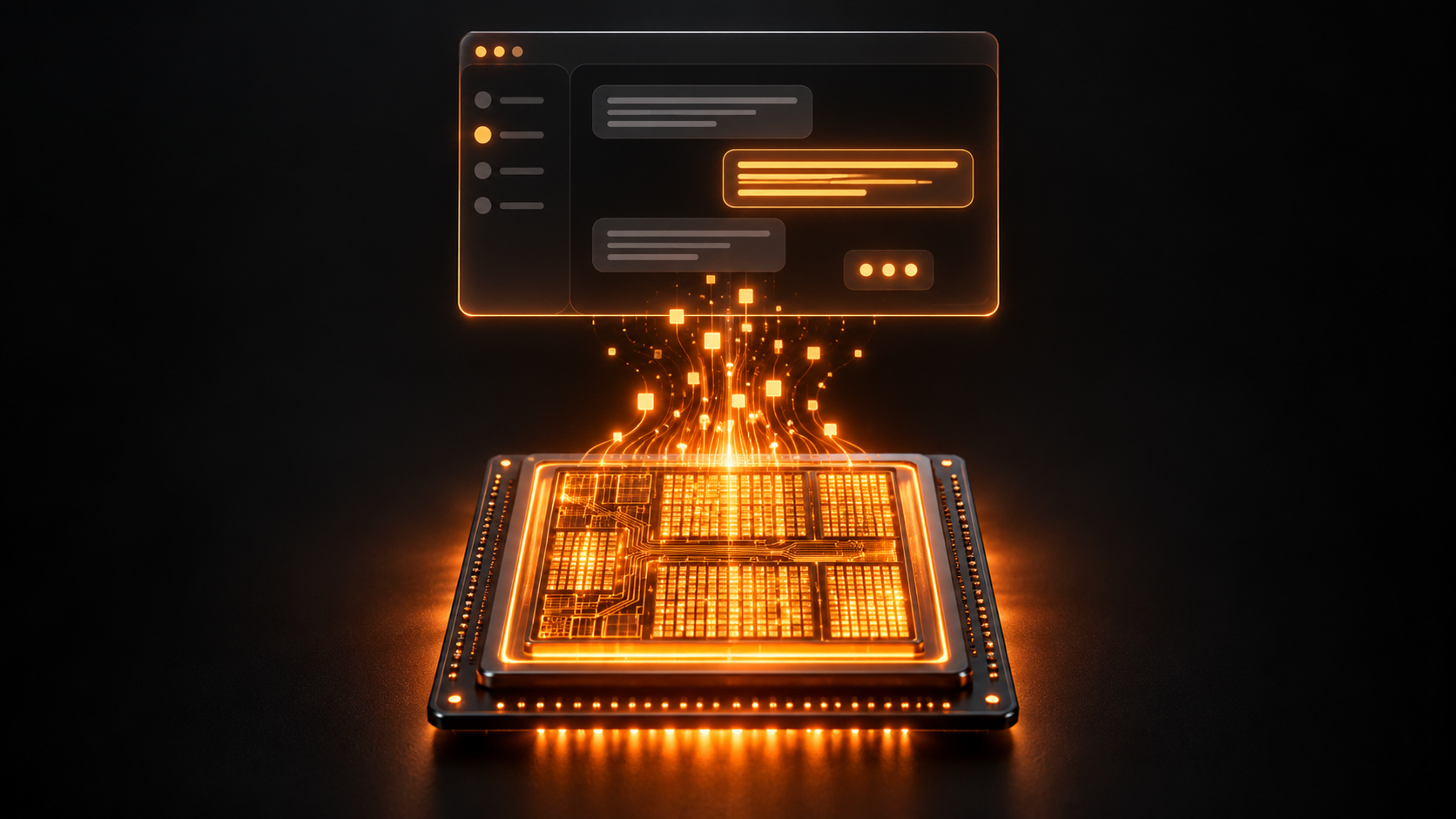
Modern AI inference has a surprisingly physical bottleneck: moving model weights around is expensive.
Large language models contain billions of parameters that must be accessed repeatedly during token generation. On conventional accelerators such as NVIDIA GPUs or AMD Instinct accelerators, those weights are stored in memory and continuously moved toward the compute units performing the underlying matrix operations.
That architecture is extremely flexible, but it also requires enormous memory bandwidth, sophisticated packaging, high-bandwidth memory such as HBM, and significant amounts of power.
Canadian AI hardware company Taalas approached the problem from a radically different direction:
What if the model did not have to be loaded into the processor at all?
What if the model itself became part of the chip?
That idea is behind what are often described as LLM burners.
From Software Model to Physical Hardware
A conventional AI accelerator is designed to run many different models.
At a highly simplified level, inference looks like:
Memory → Model Weights → Compute → Token
Taalas instead builds highly specialized silicon around a specific neural network. Its architecture brings model storage and computation onto the same chip, eliminating much of the constant movement of parameters between external memory and compute. Taalas describes this approach as creating Hardcore Models—models transformed into custom silicon.
Conceptually, the pipeline becomes closer to:
Model Embedded in Silicon → Compute → Token
This is an extreme form of hardware specialization.
The trade-off is straightforward:
less programmability in exchange for potentially much higher efficiency.
A GPU can run a different model simply by loading different weights. A model-specific accelerator cannot provide that same degree of flexibility. But if one model needs to process enormous amounts of inference traffic every day, specialization starts becoming extremely attractive.
HC1: Llama 3.1 8B Burned Into Silicon
Taalas demonstrated the concept with its first platform, HC1.
HC1 is an approximately 815 mm², 53-billion-transistor chip manufactured on TSMC's 6 nm process. Its first implementation is built specifically around Llama 3.1 8B.
According to Taalas, HC1 can generate approximately:
17,000 tokens per second per user
on Llama 3.1 8B.
The model is aggressively quantized using a mixture of 3-bit and 6-bit parameters. Despite much of the implementation being hardwired, some flexibility remains: context length is configurable and LoRA adapters can be used for fine-tuning. Taalas says its second-generation silicon moves toward standardized 4-bit floating-point formats.
The company reports that its silicon Llama is nearly 10× faster, costs approximately 20× less to build, and consumes around 10× less power than the comparison systems used in its benchmark. These remain Taalas-reported figures and should therefore be treated as vendor benchmarks rather than comprehensive independent production measurements.
But even with that qualification, HC1 demonstrates a fascinating architectural idea.
Why Memory Movement Matters So Much
The interesting part of Taalas is not simply that the chip is fast.
It attacks one of the central problems in modern computing: the memory wall.
During autoregressive LLM inference, model parameters must be repeatedly accessed during token generation. Modern processors can perform mathematical operations extraordinarily quickly, but continuously supplying the required data becomes increasingly difficult.
This is one of the reasons modern AI accelerators depend on HBM, advanced packaging, large memory interfaces and enormous bandwidth.
Taalas asks a simple question:
Why keep moving the same weights if those weights rarely change?
Its architecture attempts to remove the traditional boundary between model storage and computation. Taalas specifically argues that this allows its systems to avoid technologies such as HBM, advanced packaging, 3D stacking and high-speed external memory interfaces that are normally required by large AI accelerators.
The optimization target is therefore fundamentally different.
GPUs optimize for generality.
LLM burners optimize for executing a particular model extremely efficiently.
The Economics Become Interesting at Scale
For experimentation, training, fine-tuning and rapidly evolving models, GPUs remain the obvious choice.
Production inference, however, is increasingly becoming a different kind of computing problem.
Imagine a widely deployed model generating trillions of tokens.
At that scale, even relatively small improvements in watts per token, latency per token or cost per token can translate into enormous infrastructure savings.
A future AI datacenter could therefore become increasingly heterogeneous:
GPUs → training → fine-tuning → new models → flexible inference
Model-specific silicon → mature models → enormous inference volume → ultra-low latency → optimized cost per token
This pattern has appeared repeatedly throughout computing history.
General-purpose processors dominate while workloads are new and rapidly changing. Once particular workloads become sufficiently large and predictable, increasingly specialized hardware appears.
Bitcoin mining followed a particularly visible progression:
CPU → GPU → FPGA → ASIC
AI inference may develop its own version:
CPU → GPU → AI Accelerator → Model-Specific Silicon
Not every model needs an ASIC.
But some of the world's most heavily used models eventually might.
Why This Could Matter Even More for AI Agents
The most interesting implication may not actually be faster chatbot responses.
It could be inference-time compute.
Modern reasoning systems and AI agents increasingly perform substantial computation before producing a final response.
An agent might:
Plan → Reason → Call Tool → Observe → Critique → Reason Again → Answer
A sufficiently complex workflow can involve thousands or tens of thousands of generated tokens.
At a few hundred tokens per second, extensive reasoning introduces noticeable latency.
At thousands or potentially tens of thousands of tokens per second, the economics and user experience begin to change.
Agents could potentially perform far more planning, simulation, verification and internal reasoning while still appearing responsive in real time.
This means that specialized inference hardware could influence not only how quickly AI produces an answer, but how much computation an AI system can economically perform before producing that answer.
That may ultimately be the more important implication.
The Fundamental Weakness
There is, however, an obvious problem.
AI models evolve faster than semiconductor manufacturing.
A GPU can run a newly released model almost immediately.
A model-specific chip cannot simply download a completely different checkpoint.
If millions of dollars are invested in hardware optimized around one model and a substantially better architecture appears shortly afterwards, the economic advantage can disappear quickly.
Taalas attempts to address this problem through a design and manufacturing process intended to convert a new AI model into custom silicon in approximately two months, rather than designing an entirely new accelerator architecture for every model.
That is remarkably fast for custom silicon.
But it still means model-specific hardware makes the most sense when several conditions align:
The model is relatively stable.
Inference volume is enormous.
The efficiency gains justify dedicated manufacturing.
This is why LLM burners are unlikely to simply replace GPUs.
They are more likely to become another layer of the AI compute stack.
From Taalas Experiment to AMD Strategy
The concept received perhaps its strongest validation on August 6, 2026.
AMD announced a definitive agreement to acquire Taalas, describing the company as a pioneer in specialized AI inference silicon.
More importantly, AMD did not describe Taalas simply as an isolated accelerator company.
AMD stated that it plans to integrate Taalas technology into its AI accelerator roadmap and develop system-level solutions combining the technology with AMD Instinct GPUs.
That points toward an interesting future for AI infrastructure.
Rather than choosing between programmable GPUs and specialized silicon, datacenters could combine both:
Flexible accelerators for rapidly changing models and general AI computation.
Highly specialized silicon for models operating continuously at massive scale.
The future of AI compute may therefore not be:
GPU vs. ASIC
but rather:
GPU + ASIC
with programmable accelerators handling the rapidly changing frontier while model-specific silicon generates enormous volumes of inference underneath it.
HC1 is still fundamentally a technology demonstrator, and many questions around scaling, economics, independent efficiency measurements and support for substantially larger models remain unanswered. Taalas itself describes HC1 as its technology demonstrator and has outlined HC2 as a higher-density second-generation platform intended for more capable models.
But AMD's acquisition makes the experiment considerably more important.
If the architecture scales while retaining its performance, power and cost advantages, LLM burners could become a genuine new category of AI inference hardware.
References
1. Taalas — HC1 Technology Demonstrator / Products Official HC1 specifications, Llama 3.1 8B implementation, TSMC 6 nm process, 815 mm² die, 53B transistors and reported 17,000 tokens/s/user. Taalas — HC1 Products
2. Ljubisa Bajic, Taalas — “The Path to Ubiquitous AI” (2026) Technical overview of Taalas' Hardcore Model architecture, memory-compute integration, HC1 performance claims, quantization, LoRA support, model-to-silicon turnaround and HC2 roadmap. Taalas — The Path to Ubiquitous AI
3. AMD — “AMD Acquires Taalas to Advance Compute Solutions for Rapidly Growing AI Inference Market” (August 6, 2026) Official AMD announcement covering the definitive acquisition agreement and AMD's intention to integrate Taalas technology with its accelerator roadmap and AMD Instinct GPUs. AMD — Taalas Acquisition Announcement
4. AMD Newsroom — Artificial Intelligence / Corporate Announcements (2026) AMD's broader AI infrastructure announcements and positioning of the Taalas acquisition within its evolving AI compute portfolio. AMD AI Newsroom
Performance and efficiency figures attributed to Taalas are vendor-reported unless explicitly stated otherwise. Independent, large-scale benchmarking of the architecture remains limited as of September 2026.